Semiconductor Today Reports Our Latest PCSEL Research Progress
In February 2024, our team achieved a major advance in photonic crystal surface-emitting lasers (PCSELs), introducing a triple-lattice structure and realizing a low-threshold 1550 nm PCSEL. The results were published in Light: Science & Applications, Vol. 13, Article 44 (2024). The internationally recognized semiconductor magazine Semiconductor Today featured the work in a News Feature titled “Triple-lattice photonic crystal laser.” The report noted: “Light around 1.55 µm experiences minimal transmission loss in optical fibers and allows higher eye-safe power. Conventional lasers in this band suffer strong interband absorption and therefore poorer performance. PCSEL structures provide strong optical feedback to overcome this limitation, lowering threshold and increasing output power.”
Headquartered in the UK, Semiconductor Today is a widely recognized industry magazine focused on global semiconductor research advances and the latest industry developments.
Semiconductor Today report screenshot
A PCSEL uses a two-dimensional photonic crystal as the resonant cavity and relies on diffraction of band-edge modes to achieve surface emission. Because these modes typically have large mode areas, PCSELs exhibit a smaller far-field divergence angle than conventional communication lasers such as VCSELs and DFB lasers. In addition, PCSELs form their cavity via in-plane feedback from the 2D photonic crystal, eliminating the need for the dozens of epitaxial DBR pairs required by VCSELs for vertical feedback. These characteristics make PCSELs highly competitive in performance and cost.
However, key challenges remain, including large device size and high threshold current. A high threshold current increases power consumption and limits modulation speed. This limitation arises from the distributed-feedback mechanism of 2D photonic crystal cavities, which requires a large number of lattice periods to provide sufficiently strong optical feedback. This makes it difficult to shrink the cavity and reduce the threshold.
In photonic crystal lasers, smaller cavities lead to greater optical leakage and thus higher modal loss. Among cavity designs, the triple-lattice photonic crystal structure offers a unique advantage by delivering the lowest optical loss for the same cavity size. In this work, we propose a triple-lattice photonic crystal to enhance in-cavity feedback and demonstrate a continuous-wave, electrically pumped InP-based PCSEL operating at 1.55 μm. This provides a new route to shrinking cavity size and lowering threshold, with significant potential for high-speed optical communications, LiDAR, and related applications.
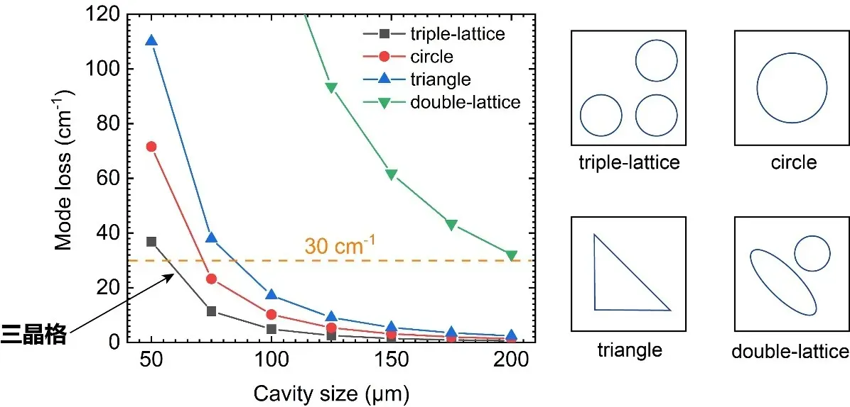
Mode loss for different photonic crystal cavities. Source: Light: Science & Applications
If we call a photonic crystal with a single hole per unit cell a single-lattice crystal, then a triple-lattice cavity can be regarded as a structural nesting of three single-lattice crystals. By adjusting the relative offsets between these lattices, effects unreachable with a single lattice can be achieved. In this report, the lattice offset was set to half a wavelength so that the round-trip feedback path becomes an integer multiple of the wavelength, enabling constructive interference. From the perspective of coupled-wave theory, optical feedback strength is governed by coupling between 180° counter-propagating waves and depends on the second-order Fourier component of the refractive index distribution. Our study reveals its functional dependence on lattice offset. Compared with a single lattice, the triple lattice can provide up to a threefold enhancement in 180° optical feedback, suppressing lateral leakage and enabling smaller cavities and lower thresholds.
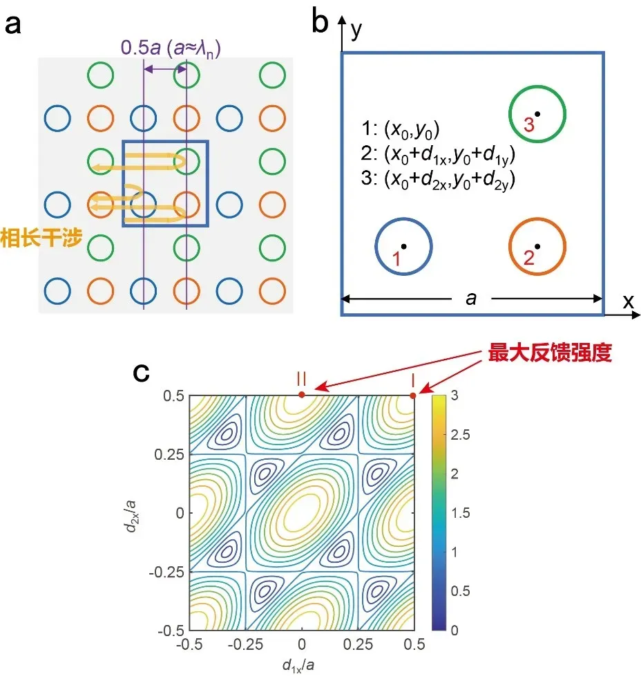
Working mechanism of the triple-lattice photonic crystal cavity. Source: Light: Science & Applications
The device adopts an all-semiconductor structure compatible with conventional DFB processing and is fabricated using MOCVD regrowth. The epitaxial stack, including multiple quantum wells, is first grown on an InP substrate. Electron-beam lithography and dry etching are then used to define sub-100-nm photonic crystal holes. Finally, a second epitaxial regrowth fills the holes and overgrows a p-doped layer to complete the device.
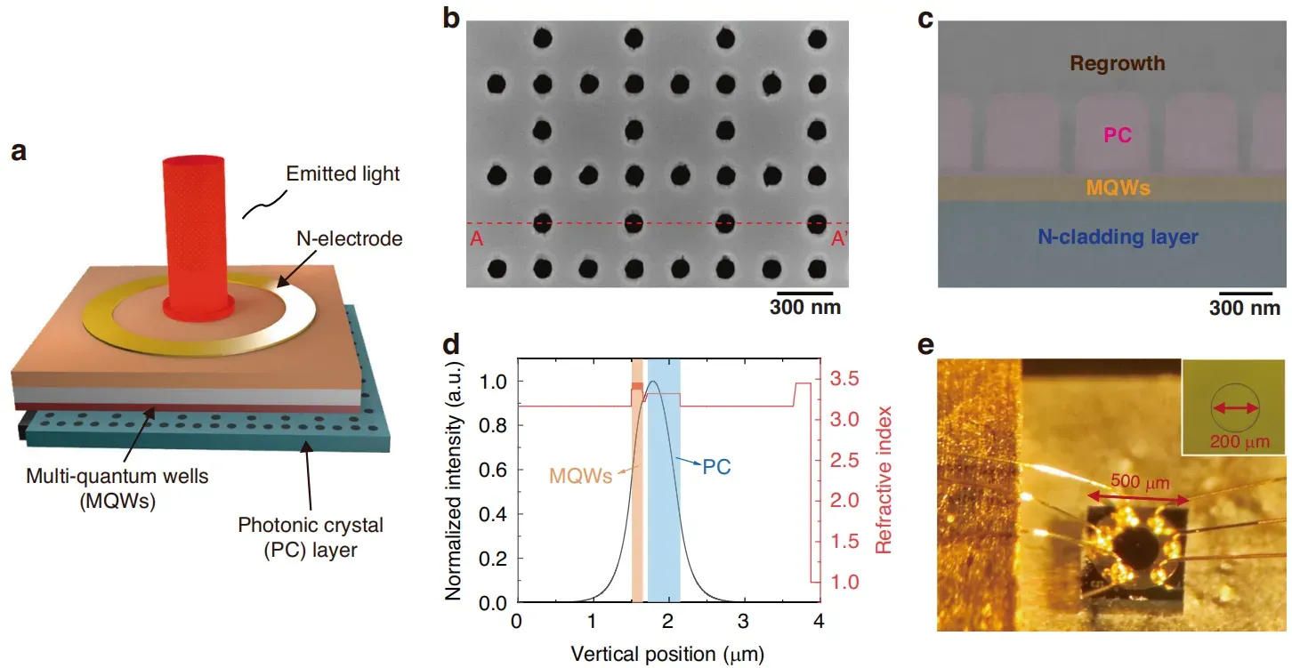
1550 nm triple-lattice PCSEL device structure. Source: Light: Science & Applications
As a core operating characteristic, the device shows a stable lasing peak at 1.55 μm under continuous-wave operation, in excellent agreement with the designed Γ2 band-edge mode. Notably, no parasitic resonances were observed over a broad spectral scan (1350–1650 nm), confirming that the triple-lattice structure successfully locks the oscillation mode to the target band.
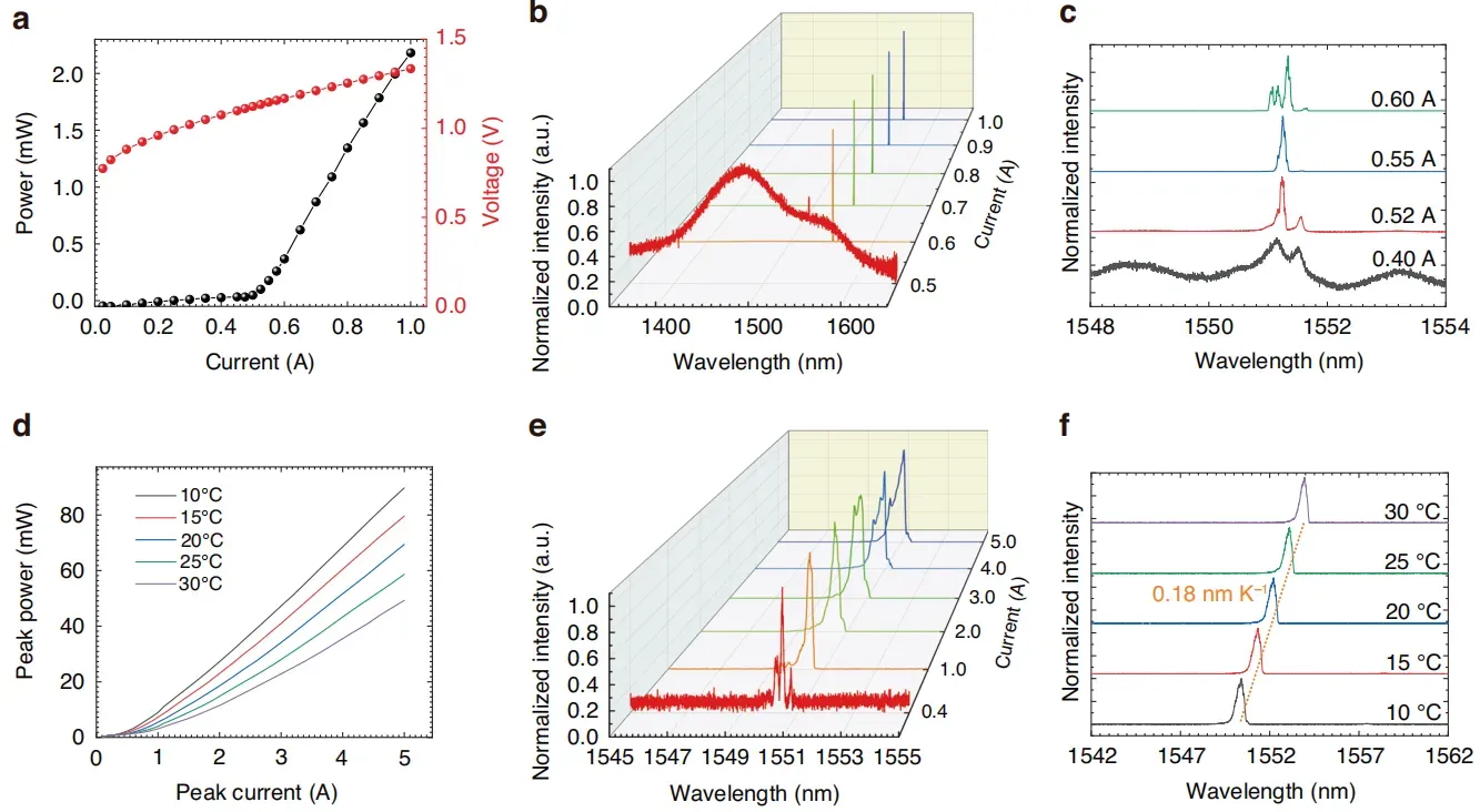
1550 nm triple-lattice PCSEL operating characteristics. Source: Light: Science & Applications
PCSELs are a major focus in the semiconductor laser community and can be applied to optical communications, laser pumping, sensing, and medical systems. Yet, large device size and high threshold current still limit practical adoption in high-speed optical communications. In this work, we introduce a new triple-lattice photonic crystal cavity and demonstrate a continuous-wave, electrically pumped 1.55 μm PCSEL based on this structure. We believe the results open a new path toward smaller, lower-threshold PCSELs and can enable future applications in high-speed optical communications. The work also deepens our understanding of feedback mechanisms in photonic crystal cavities and provides new degrees of freedom for cavity design.
Related Links
[1] Paper: https://doi.org/10.1038/s41377-024-01387-4
[2] Semiconductor Today report: https://semiconductor-today.com/news_items/2024/feb/ucas-230224.shtml
Need full specs and pricing?
Contact our engineering team for datasheets and application support.