Our Project Wins the National Disruptive Innovation Competition Award
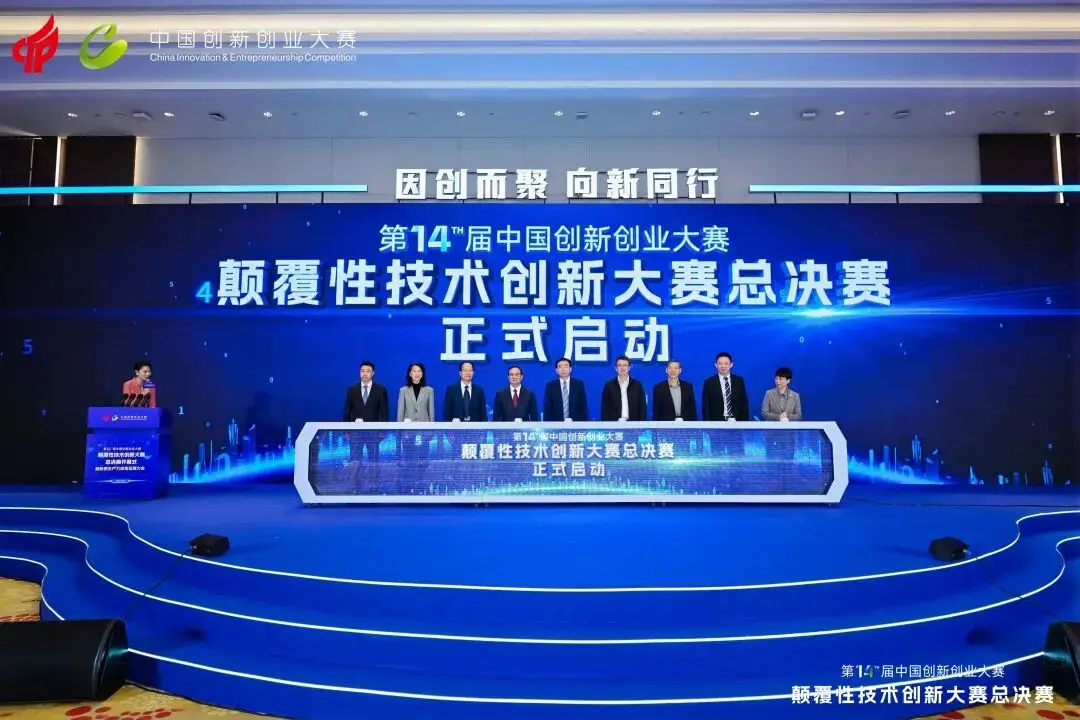
From December 10–12, 2025, the National Finals of the 14th China Innovation & Entrepreneurship Competition – Disruptive Technology Innovation Track were held in Shangcheng District, Hangzhou. The event was organized by the Torch High Technology Industry Development Center of the Ministry of Industry and Information Technology, and co-hosted by the Hangzhou Municipal People’s Government, the Zhejiang Provincial Department of Economy and Information Technology, and the Zhejiang Provincial Department of Science and Technology.
Our independently developed “High-Performance Photonic Crystal Laser” project advanced through open selection, sector competitions, and the national finals, ultimately winning the Outstanding Award—the top honor of the competition.
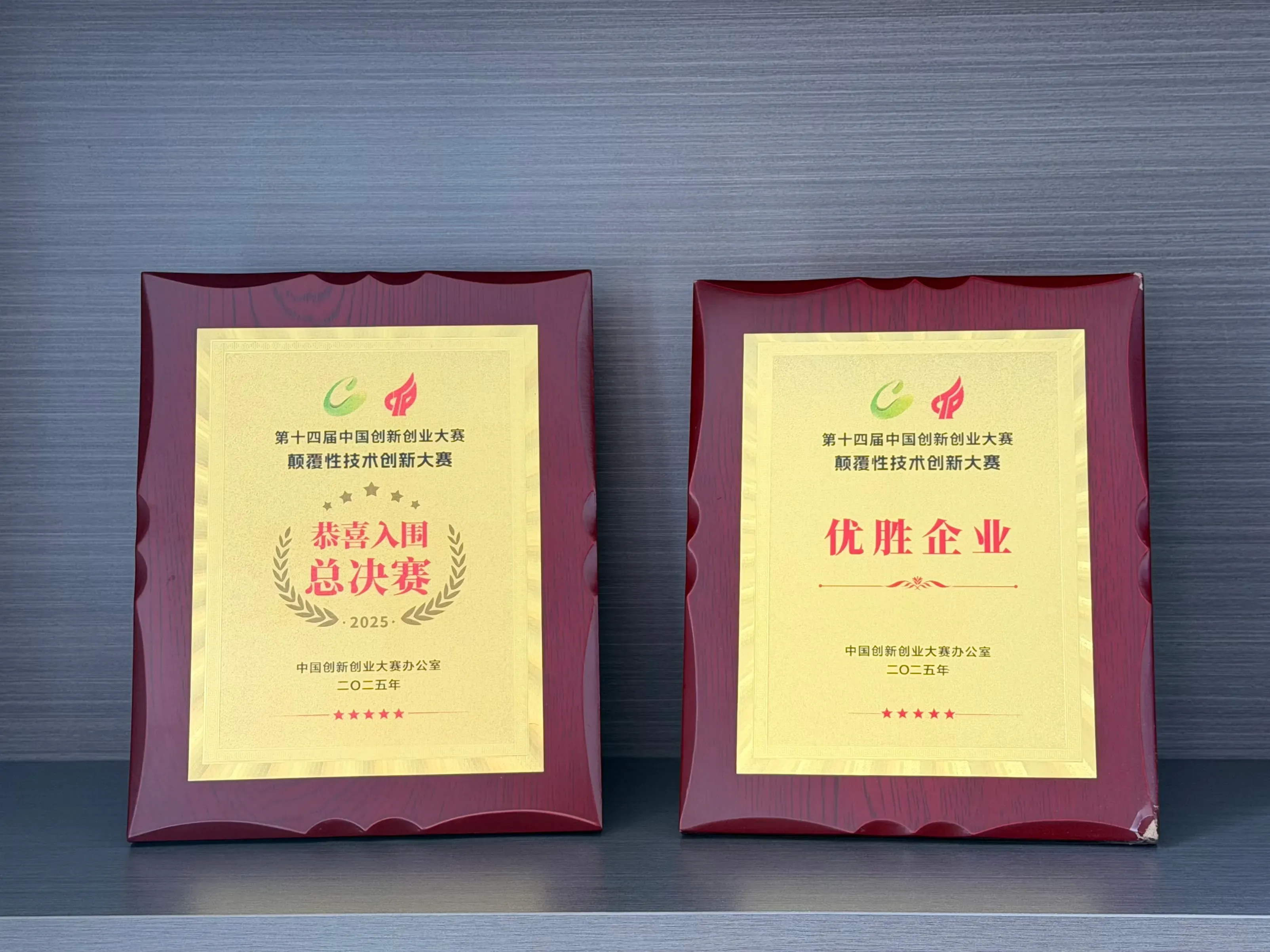
Hangzhou GCLight Semiconductor Co., Ltd. received the award
Since its launch in August 2025, the competition attracted 891 high-quality projects nationwide across six frontier fields: future materials, future manufacturing, future information, future energy, future space, and future health. After multiple rounds of evaluation, 163 disruptive technology projects advanced to the national finals.
The competition was highly competitive, with expert judges from industry, investment institutions, and the research community evaluating originality, engineering maturity, and market outlook. Our project’s success underscores its disruptive technology capability, engineering execution, and long-term growth potential in the laser field.
Photonic crystal lasers, as a key next-generation semiconductor laser technology, can simultaneously deliver high power, small divergence, and narrow linewidth. They can break conventional semiconductor laser limits, enabling single-chip output above 100 W with divergence below 1°. This technology has disruptive impact in intelligent sensing, biomedical applications, LiDAR, optical pumping, and quantum technologies. Our project focuses on core chip design, device structure optimization, and engineering implementation, establishing a complete and independent technology roadmap.
This award not only recognizes the project’s technical advancement and commercial value, but also marks a milestone in our progress toward high-end laser sources. Going forward, we will continue to invest in R&D, accelerate product engineering and industrialization, and advance large-scale adoption of high-performance domestic laser technologies to support high-quality growth in China’s optoelectronics industry.
Need full specs and pricing?
Contact our engineering team for datasheets and application support.
GC Light Achieves 200 mW Room-Temperature CW Output from a 1.3 μm Quantum-Dot PCSEL
GC Light has raised the room-temperature CW output power of its reported 1.3 μm InAs/GaAs quantum-dot PCSEL to 200 mW, setting a new benchmark among comparable 1.3 μm devices.
What Is PCSEL: The Next-Generation High-Performance Semiconductor Laser
A technical overview of PCSELs (photonic crystal surface-emitting lasers), explaining their operating principles and advantages in brightness, linewidth, and beam shaping.