First Room-Temperature CW Operation of a 1.3 μm Quantum-Dot PCSEL
With rapid advances in optical communications, LiDAR, and silicon photonics, there is a growing demand for high-performance, low-cost light sources with small divergence. Photonic crystal surface-emitting lasers (PCSELs), leveraging band-edge resonance in photonic crystals, support in-plane resonance and vertical emission, offering large single-mode areas, high power, and narrow divergence. They are widely regarded as a promising next-generation high-brightness source.
Scalable PCSEL deployment hinges on efficient coupling between the gain medium and the resonant structure. In recent years, InAs/GaAs quantum dots (QDs) have emerged as a compelling gain platform due to their excellent high-temperature performance in the O-band (~1310 nm) and potential compatibility with GaAs and silicon processing. Compared with conventional InP-based quantum wells, QDs can deliver high performance at lower cost, aligning well with silicon photonics requirements for cost and reliability.
However, QD-PCSEL development faces key challenges: a thin QD gain region, a low optical confinement factor, and slow carrier relaxation reduce modal gain. If cavity loss is high, lasing cannot be achieved. While buried-heterostructure PCSELs in quantum-well systems have demonstrated watt-class CW output, QD PCSELs have not achieved room-temperature CW operation to date. The bottleneck is the need to markedly reduce cavity loss so that the gain can reach threshold.
To address this, our team introduced a triple-lattice photonic crystal structure. By precisely offsetting air holes within the lattice, we maintain low fundamental-mode loss while improving vertical radiation efficiency. This enables the first room-temperature continuous-wave lasing of an InAs/GaAs QD PCSEL within a compact 100×100 μm photonic-crystal cavity.

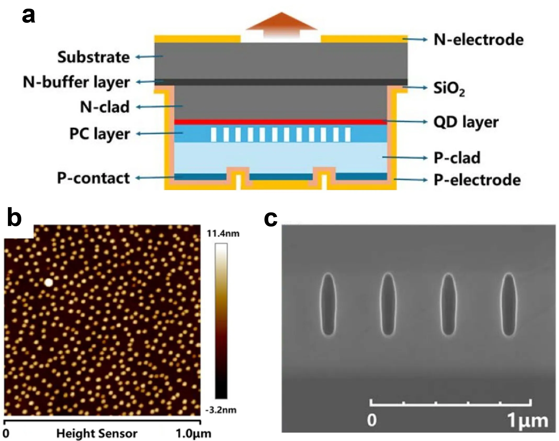
Device structure of the 1.3 μm triple-lattice QD PCSEL. Source: Optics Express
Achieving efficient QD–photonic crystal coupling and room-temperature CW lasing requires precision growth and nanofabrication, including active-region growth, photonic crystal etching, and regrowth.
First, multiple layers of InAs/InGaAs QD DWELL structures are grown on GaAs substrates by molecular beam epitaxy (MBE). A 300 nm p-GaAs layer is then regrown as the etch layer for the photonic crystal. Electron-beam lithography defines the triple-lattice photonic crystal over a 100×100 μm area, followed by ICP dry etching to form high-aspect-ratio air holes. Metal-organic chemical vapor deposition (MOCVD) regrowth creates an asymmetric waveguide structure. Finally, photolithography defines a circular mesa for current confinement, a SiO2 passivation layer is deposited and opened, and metal contacts are formed.
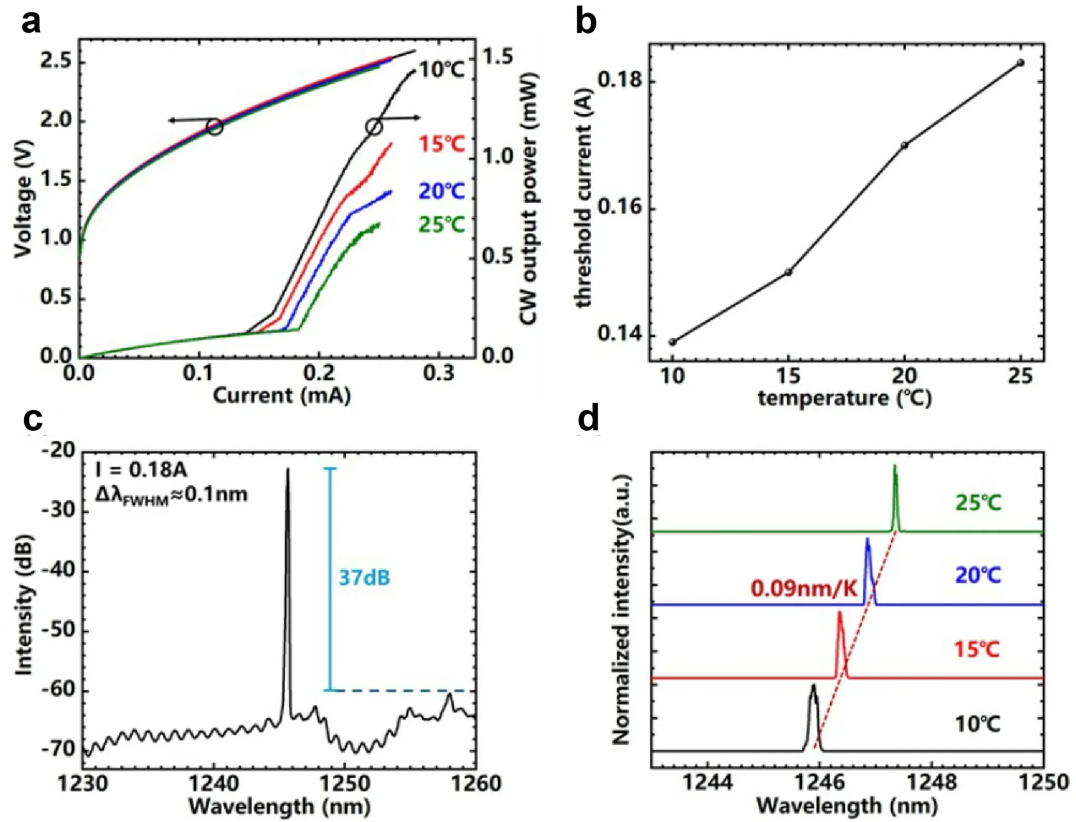
Operating characteristics of the 1.3 μm triple-lattice QD PCSEL. Source: Optics Express
Using this approach, the QD photonic crystal laser achieved a threshold current of 139 mA and output power exceeding 1.4 mW at 10°C, with a side-mode suppression ratio of 37 dB and a spectral linewidth of ~0.1 nm, demonstrating good single-mode behavior. The wavelength temperature drift is 0.09 nm/K. Proton implantation can further reduce the threshold to 80 mA. Current performance is mainly limited by thermal and electrical resistance; further improvements in spectral matching, heat dissipation, and injection design are expected to enhance power and efficiency.
This breakthrough validates the feasibility of integrating QDs with PCSELs and establishes a critical foundation for high-performance, low-cost 1.3 μm surface-emitting lasers. With continued advances in structure design, materials growth, and process integration, QD PCSELs are poised to impact data-center interconnects, sensing, and imaging, accelerating silicon photonics integration.
Related Links
[1] Paper: https://doi.org/10.1364/oe.562475
Need full specs and pricing?
Contact our engineering team for datasheets and application support.